 Electronics
 Switching Power Supply EMI Suppression Tips: Stop Your Circuit from Interfering with Others
Why Your Switching Power Supply Keeps Interfering with Others
Switching power supplies are efficient and compact, but EMI (Electromagnetic Interference) issues have always been a headache. A poorly filtered Buck circuit can cause the entire 2.4GHz band noise to spike, leading to WiFi disconnections, Bluetooth dropouts, and ADC readings jumping around… These are real-world failure scenarios.
EMI is not mysticism - it has clear generation mechanisms and suppression methods. Master a few key techniques, and your design can go from “failing certification” to “passing on the first try.”
Where Does EMI Come From?
EMI from switching power supplies mainly comes from two sources:
Differential-mode interference: Interference generated by current flowing back and forth in the power loop. Frequency is relatively low (150kHz~30MHz), mainly propagating through conduction.
Common-mode interference: Parasitic capacitance coupling from switching transistors to ground causes noise current to return through the ground line. Frequency is higher (30MHz~1GHz), mainly propagating through radiation.
Simply put: low frequency propagates through conduction, high frequency through radiation. Suppression strategies must also be divided accordingly.
Tip #1: Input Filtering
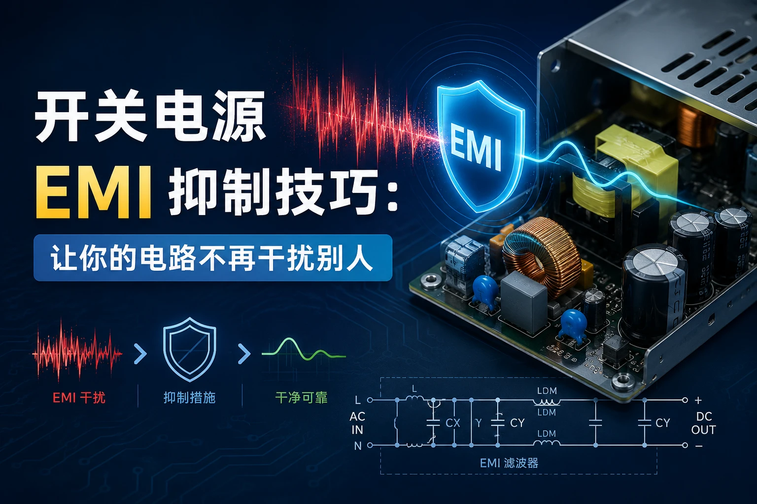
Input filtering is the first line of defense for EMI suppression. A basic LC filter can attenuate most switching frequency harmonics.
Practical circuit:
Vin o----+----o Vout
         |
        +-+
        | | Cx (X2 safety capacitor, 1μF)
        +-+
         |
        ~~~ Common-mode choke (CM choke)
        ~~~
         |
        +-+
        | | Cy (Y capacitor, 2.2nF)
        +-+
         |
        GND
Component selection key points:
-
X2 capacitor: Connected between L-N, absorbs differential-mode noise. Choose 0.47μF~1μF, voltage rating above 275VAC.
-
Common-mode choke: Presents high impedance to common-mode noise, basically no effect on differential-mode signals. Choose 2.2mH~10mH, rated current should have margin.
-
Y capacitor: L/N to ground, filters out common-mode noise. Note that Y capacitor value cannot be too large, otherwise leakage current will exceed standards. Generally 1nF~4.7nF.
Actual measurement data: A 12V/3A Buck converter without filtering has conducted EMI exceeding standards by 15dB; after adding LC filtering, margin is 8dB, easily passing CISPR 32 Class B.
Tip #2: PCB Layout
PCB layout’s impact on EMI is much greater than many people imagine. The same circuit with different layouts can have EMI results differing by 20dB.
Key principles:
- Minimize switching loop area
The high di/dt loop formed by the switching transistor, inductor, and input capacitor should have the smallest area possible. This loop is an antenna - the larger the area, the stronger the radiation.
❌ Wrong: Input capacitor far from switching transistor, large loop area
✅ Correct: Input capacitor close to switching transistor pins, compact loop- Maintain ground plane integrity
Don’t route traces or create slots on the ground plane. A complete ground plane provides low-impedance return paths, reducing radiation.
- Adequately ground the thermal pad
The thermal pad at the bottom of the IC must be well grounded. It not only dissipates heat but also serves as a shield. Use a dense via array to connect to the ground plane.
Layout checklist:
| Check item | Requirement |
|---|---|
| Switching loop area | < 1cm² |
| Ground plane splitting | Avoid splitting, maintain integrity |
| Thermal pad vias | ≥ 6, diameter 0.3mm |
| Feedback traces | Keep away from switching nodes, route on inner layers |
| Output capacitor | Place close to load |
Tip #3: Snubber Circuit
Ringing at the switching node is a major source of high-frequency EMI. Parasitic inductance and parasitic capacitance form LC resonance, producing oscillations from tens to hundreds of MHz.
RC Snubber is the simplest and most effective suppression method:
Switching node o----+----o
                    |    |
                   Rsn  Csn
                    |    |
                    +----+
                    |
                   GND
Parameter calculation:
-
Rsn ≈ √(Lparasitic / Cparasitic), typically 10Ω~100Ω
-
Csn ≥ 10 × Cparasitic, typically 100pF~1nF
Debugging tips: Use an oscilloscope to view the switching node waveform. After knowing the ringing frequency f_ring, choose Csn to make the snubber resonance frequency slightly lower than the ringing frequency. Start tuning from 47Ω + 470pF, optimizing step by step.
Tip #4: Spread Spectrum Modulation
If your power supply chip supports it, enable the Spread Spectrum Modulation (SSM) function.
The principle is simple: periodically dither the switching frequency within a small range (e.g., ±2%), spreading the energy concentrated at a single frequency across a frequency band. Peak noise is reduced by 10~15dB.
# Taking TPS54331 as an example, implement spread spectrum through external clock source
# Refer to the "Spread Spectrum" section in the chip datasheet for specific configuration
# Usually just requires setting a pin level or modifying a register
Not all chips support this, but if you’re using mid-to-high-end models from major manufacturers like TI, MPS, Diodes, etc., there’s a high probability this feature is available.
Tip #5: Shielding
When filtering and layout are both done well, but you’re still a few dB short of margin? Add shielding.
Practical solutions:
-
Inductor shielding: Use shielded power inductors, which have 10~20dB lower radiation than unshielded inductors.
-
PCB shielding cans: Metal shielding cans placed over the switching power supply area, soldered to the ground plane at the bottom. Cost increase is minimal, effect is immediate.
-
Ferrite beads: Put ferrite rings on output cables to suppress cables becoming radiation antennas.
Cost reference:
| Shielding solution | Unit cost | Application scenario |
|---|---|---|
| Shielded inductor | ¥0.5~2 | All switching power supplies |
| Ferrite ring | ¥0.3~1 | Modules with cable output |
| Metal shielding can | ¥2~8 | High-density, high-requirement products |
| Conductive foam | ¥1~3 | Enclosure gap shielding |
Tip #6: Soft Switching Technology
If the above methods are still not enough, consider solving the problem at the topology level.
Zero Voltage Switching (ZVS) and Zero Current Switching (ZCS) allow switching transistors to switch when voltage or current is zero, fundamentally eliminating switching noise.
Implementation methods:
-
Resonant converters: LLC topology, efficiency can reach 95%+, EMI is extremely low
-
Active clamp: Add active clamp circuit to flyback topology
-
GaN/SiC devices: Although switching speed is fast, with correct drive and layout, overall EMI is actually lower (because di/dt is controllable)
Of course, the tradeoff is increased design complexity. For consumer products, the previous tips are usually sufficient.
Common Problem Troubleshooting
Q1: Conducted EMI exceeds standards at 150kHz~500kHz
A: Differential-mode noise is the main issue. Increase X2 capacitor or add another stage of LC filtering. Check if the input capacitor’s ESR is too low.
Q2: Radiated EMI exceeds standards at 30MHz~100MHz
A: Common-mode noise. Check if the common-mode choke direction is correct (two windings wound in the same direction), and if Y capacitors are properly connected.
Q3: Radiated EMI exceeds standards at 100MHz~300MHz
A: Switching node ringing. Add RC snubber, shorten switching node traces, check PCB stackup design.
Q4: Spikes at specific frequency bands
A: May be harmonics of the switching frequency. Confirm switching frequency setting is correct, try enabling spread spectrum function.
Q5: Prototype testing OK, but batch products fail EMI
A: Component tolerances cause filtering parameter drift. Check inductor saturation current, capacitor tolerance, use ±10% precision components at critical positions.
Summary
EMI suppression doesn’t rely on luck, but on systematic design process:
-
First do input filtering well - X2 capacitor + common-mode choke + Y capacitor, this is the first line of defense
-
Optimize PCB layout - minimize switching loop area, maintain ground plane integrity, adequately ground thermal pads
-
Add RC Snubber to absorb switching node ringing, eliminating the main source of high-frequency EMI
-
When necessary, use spread spectrum modulation and shielding measures to further reduce peak noise
Following this sequence to check item by item, most EMI problems can be solved. Remember: spending one more hour at the schematic stage is better than spending three days in the test lab.
Hope this blog post is helpful to you!