 Embedded Development
 CH569/CH565 Deep Dive: RISC-V Core + USB 3.0 SuperSpeed — The Complete Guide to China's High-Speed Interface MCU
When embedded engineers hear “WCH” (沁恒), the first thing that comes to mind is usually the CH340 USB-to-serial chip or the CH32V series of general-purpose RISC-V MCUs. But WCH also has a truly unique flagship chip — the CH569/CH565.
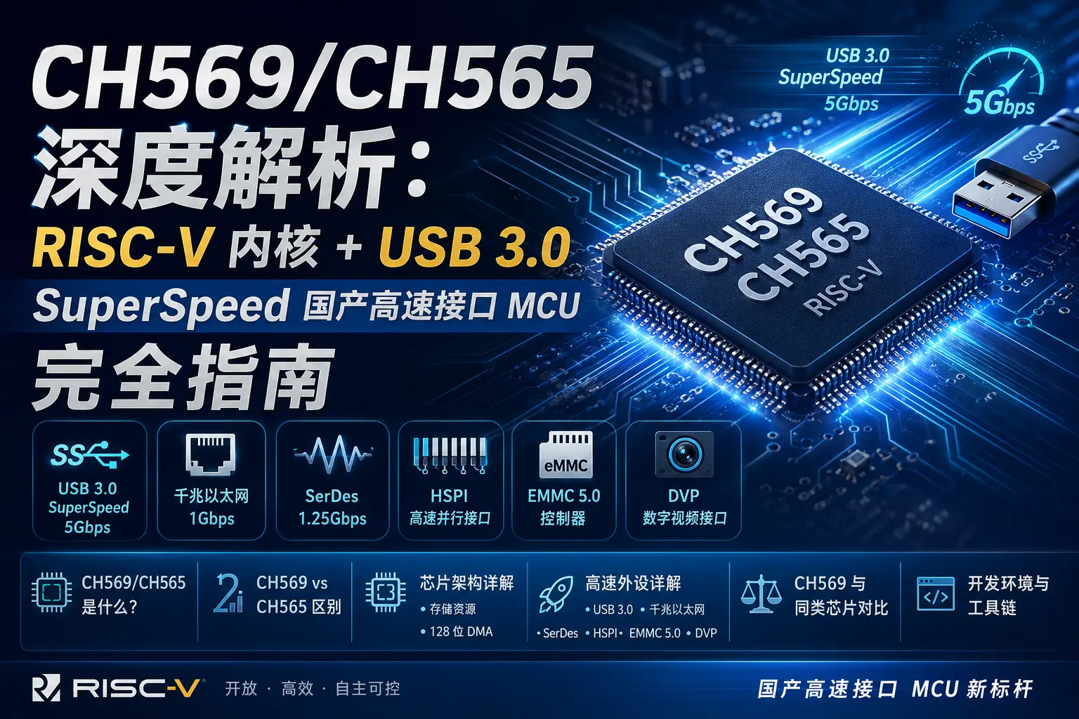
It is the world’s first RISC-V MCU with a built-in USB 3.0 PHY, while also integrating Gigabit Ethernet, SerDes fiber-optic direct drive, HSPI high-speed parallel interface (3.8Gbps), an EMMC controller, and a hardware AES/SM4 encryption/decryption module. In this article, we’ll break down the technical details, development environment, and hands-on usage of this chip all in one go.
1. What Are the CH569/CH565?
The CH569 and CH565 are 32-bit RISC-V high-speed interface MCUs from WCH, based on their proprietary RISC-V3A core. They support the IMAC instruction subset (integer, multiply, atomic, compressed instructions), run at 120MHz, and use a low-power two-stage pipeline.
The biggest selling point of these chips isn’t raw compute — a 120MHz RISC-V core in 2026 is hardly top-of-the-line. The real killer feature is the built-in high-speed interface PHYs:
- USB 3.0 SuperSpeed (5Gbps) — integrated PHY, no external USB 3.0 transceiver needed
- Gigabit Ethernet — integrated MAC + RGMII/RMII PHY interface
- SerDes (1.25Gbps) — integrated PHY, can directly drive fiber optics
- HSPI high-speed parallel interface — 8/16/32-bit configurable, up to 3.8Gbps
- EMMC 5.0 — supports 1-line / 4-line / 8-line modes
- DVP digital video interface — 8/10/12-bit, supports YUV/RGB/JPEG
In the embedded chip space, it’s extremely rare to find an MCU that integrates this many high-speed PHYs. Typically you’d need an FPGA or an expensive SoC to get comparable interface density.
2. CH569 vs CH565 Differences
The CH569 and CH565 use the same silicon die — the only difference is package and IO count:
| Parameter | CH569 | CH565 |
|---|---|---|
| Package | QFN68 (8×8mm) | QFN40 (6×6mm) |
| GPIO | 49 pins | ~30 pins |
| HSPI max bus width | 32-bit | 16-bit |
| Core / Clock / Memory / All high-speed interfaces | Identical | Identical |
Simply put: the CH569 is the full version, the CH565 is the compact-package version. If you don’t need 32-bit HSPI or 49 GPIOs, the QFN40 CH565 saves PCB area and cost.
3. Chip Architecture Explained
3.1 Processor Core
- Core: RISC-V3A (WCH proprietary), RV32IMAC instruction set
- Clock: 120MHz
- Pipeline: Two-stage, low-power design
- Hardware divider: Single-cycle multiply, hardware division
- Interrupt controller: Programmable, supports nested interrupts
While 120MHz doesn’t match the ESP32-S3 (240MHz) or STM32H7 (480MHz), the CH569 isn’t positioned for general-purpose compute — it’s designed for high-speed data movement. The 128-bit-wide DMA bus is the real star.
3.2 Memory Resources
CodeFlash:  448KB  (program storage)
DataFlash:   32KB  (data storage)
SRAM (32-bit):  16KB  (system SRAM)
SRAM (128-bit): 32/64/96KB configurable  (high-speed data buffer)
The 96KB of 128-bit-wide SRAM is key — it sits directly on the 128-bit DMA bus and serves as the data buffer for USB 3.0, HSPI, EMMC, and other high-speed peripherals. At 120MHz, the theoretical bandwidth of the 128-bit bus is approximately 1.92GB/s, far exceeding the needs of any single peripheral, ensuring DMA is never the bottleneck.
3.3 128-bit DMA
This is the most critical design element of the CH569 architecture. The 128-bit DMA controller connects all high-speed peripherals:
                  ┌────────────────────┐
                  │   128-bit DMA Bus   │
                  │   (≈1.92GB/s)       │
                  └───┬──┬──┬──┬──┬─────┘
                      │  │  │  │  │
                 ┌────┘  │  │  │  └────┐
                 ▼       ▼  ▼  ▼       ▼
              USB3.0   HSPI EMMC SerDes ETH
             (5Gbps)  (3.8 (eMMC (1.25 (1Gbps)
                       Gbps)5.0) Gbps)
All high-speed peripheral data transfers are handled automatically by DMA. The CPU only needs to configure the descriptors, then move on to other tasks. This is the core reason the CH569 can handle 5Gbps USB 3.0 data with just a 120MHz core.
4. High-Speed Peripherals in Detail
4.1 USB 3.0 SuperSpeed (5Gbps)
The CH569’s USB 3.0 controller is a complete implementation with a built-in full-speed PHY — this is its biggest differentiator from other MCUs. The vast majority of MCUs only have a USB 2.0 PHY; USB 3.0 typically requires an external transceiver (such as the CYUSB3014).
Key features:
- Host / Device / OTG triple mode
- USB 3.0 HUB support (can serve as a USB 3.0 Hub controller)
- Control / Bulk / Interrupt / Isochronous transfer types
- Also includes a built-in USB 2.0 HS (480Mbps) PHY
Practical use cases:
- USB 3.0 FIFO bridge: FPGA ↔ PC high-speed data transfer
- USB 3.0 enclosure: Paired with EMMC, functions as a portable SSD
- USB 3.0 camera: Paired with DVP, transmits uncompressed video streams
The official USB 3.0 Demo’s measured throughput (from the readme): the host sends 4 burst packets to endpoint 2, then reads 4 packets back, with 4GB of data in each direction, averaged. Actual effective bandwidth typically falls in the 300–400MB/s range.
4.2 Gigabit Ethernet
Integrated Gigabit MAC supporting both RGMII and RMII PHY interfaces:
- RGMII: Connect to an external Gigabit PHY (e.g., RTL8211) for 1000Mbps
- RMII: Connect to an external 100Mbps PHY (e.g., LAN8720) for 100Mbps
The official SDK provides a complete WCHNET protocol stack, which already implements:
- TCP Server/Client
- UDP Server/Client
- DHCP client
- DNS resolution
- ICMP Ping
- MAC Raw frame send/receive
4.3 SerDes (1.25Gbps)
This is one of the CH569’s most unique peripherals. The built-in SerDes PHY can directly drive fiber-optic modules or transmit over a single twisted pair for up to 90 meters.
Key parameters:
- Speed: 1.25Gbps
- Medium: Fiber (directly drives SFP) or copper (single twisted pair, 90 meters)
- Protocol: Custom high-speed serial protocol
Application scenarios:
- Long-distance industrial cameras (90m twisted-pair video transmission)
- Board-to-board high-speed interconnect (replacing PCIe/LVDS)
- Galvanically isolated communication
4.4 HSPI High-Speed Parallel Interface
HSPI (High-Speed Parallel Interface) is the CH569’s data throughput champion:
- Bus width: 8/16/32-bit configurable
- Max speed: ~3.8Gbps (32-bit × 120MHz theoretical peak)
- Built-in FIFO + DMA
- Supports hardware encryption/decryption (AES/SM4 inline encrypt/decrypt)
The most common use for HSPI is high-speed communication with an FPGA. The 32-bit wide, 3.8Gbps bandwidth is sufficient for transmitting HD video streams or high-speed ADC sampling data.
4.5 EMMC 5.0 Controller
Full support for the EMMC 4.4/4.5.1 specification, compatible with 5.0:
- 1-bit / 4-bit / 8-bit data modes
- HS200/HS400 high-speed modes
- DMA read/write
Paired with HSPI or USB 3.0, it enables a high-speed data logger — receive data from a high-speed interface and write it to EMMC storage.
4.6 DVP Digital Video Interface
The DVP interface can directly connect to CMOS image sensors:
- 8/10/12-bit data width
- Supports YUV, RGB, and JPEG compressed data
- Combined with USB 3.0 or Ethernet, enables video streaming
4.7 Hardware Encryption/Decryption
The CH569 integrates AES and SM4 (Chinese national standard) hardware accelerators, supporting 8 encryption/decryption mode combinations. More importantly — encryption/decryption can be applied directly on the SRAM, EMMC, and HSPI data paths, enabling inline crypto operations without consuming CPU time.
5. CH569 Comparison with Similar Chips
5.1 vs General-Purpose MCUs
| Feature | CH569 | ESP32-S3 | STM32H743 | CH32V307 |
|---|---|---|---|---|
| Core | RISC-V 120M | Xtensa LX7 240M | Cortex-M7 480M | RISC-V 144M |
| USB 3.0 PHY | ✅ Built-in | ❌ | ❌ | ❌ |
| USB 2.0 HS PHY | ✅ Built-in | ❌ (FS only) | ✅ Built-in | ✅ Built-in |
| Gigabit ETH | ✅ RGMII | ❌ | ❌ (MAC only) | ❌ |
| SerDes | ✅ 1.25G | ❌ | ❌ | ❌ |
| Approx. price | ~¥25–35 | ~¥15–25 | ~¥50–80 | ~¥8–15 |
The CH569 doesn’t directly compete with general-purpose MCUs — its value lies in its built-in high-speed interface PHYs. If you don’t need USB 3.0/SerDes/HSPI, an ESP32 or CH32V307 is a more economical choice. But when you do need these interfaces, the CH569 replaces the combination of MCU + external USB 3.0 chip + SerDes chip with a single chip, significantly reducing BOM cost and PCB area.
5.2 vs Dedicated USB 3.0 Chips
| Feature | CH569 | CYUSB3014 (FX3) | FT601 |
|---|---|---|---|
| Type | Full MCU | USB 3.0 controller | USB 3.0 FIFO |
| GPIO / other peripherals | Rich | Limited | Minimal |
| Standalone operation | ✅ Yes | ❌ Requires external MCU | ❌ Requires external FPGA/MCU |
| Price | ~¥25–35 | ~¥100–150 | ~¥60–100 |
This is the CH569’s biggest competitive advantage — it’s a complete MCU that can run programs independently, unlike the FX3/FT601 which require a host controller to function.
6. Development Environment and Toolchain
6.1 MounRiver Studio
The official development environment for the CH569/CH565 is MounRiver Studio (based on Eclipse CDT), which is WCH’s unified IDE for their RISC-V MCUs.
- Download: mounriver.com
- Project format:
.wvproj(WCH-VS Project, MounRiver-specific) - Debug interface: 2-wire debug interface (similar to SWD), supports in-circuit emulation
Additionally, every example project in the official SDK includes both a makefile and makefile_rv_gcc, meaning GCC Makefile command-line builds are fully supported — MounRiver Studio is not mandatory.
6.2 Official SDK Structure
Full directory structure of the GitHub repository openwch/ch569:
ch569/
├── Datasheet/          # Datasheets
├── EVT/                # Evaluation kit
│   └── EXAM/           # Example code
│       ├── GPIO/       # GPIO input/output
│       ├── UART/       # Serial communication (up to 6Mbps)
│       ├── SPI/        # SPI master/slave modes
│       ├── TMR/        # Timers and PWM
│       ├── PWMX/       # Extended PWM
│       ├── ETH/        # Ethernet (TCP/UDP/DHCP/DNS/Ping)
│       ├── USBSS/      # USB 3.0 SuperSpeed (Host/Device)
│       ├── HSPI/       # High-speed parallel interface
│       ├── EMMC/       # EMMC storage
│       ├── DVP/        # Digital video interface
│       ├── ECDC/       # Encryption/decryption (AES/SM4)
│       ├── FLASH/      # Flash read/write
│       └── BUS8/       # 8-bit bus
└── SCHPCB/             # Dev board schematics and PCB
6.3 Development Board Options
Currently, development board options for the CH569/CH565 are limited:
- WCH official evaluation board —
CH569W-R0-1v0(QFN68) /CH565W-R0-1v0(QFN40), SCHPCB files are open-sourced on GitHub, so you can order your own PCB - Third-party minimum system boards — Available on Taobao, priced around ¥40–80
Since the CH569 uses a QFN68 package (0.4mm pitch), hand soldering is challenging. It’s recommended to purchase a ready-made development board or core board.
7. Hands-On: GPIO + UART Basics
Below, we’ll walk through the basic development workflow for the CH569 using the official SDK’s GPIO and UART examples.
7.1 GPIO Output — Blinking an LED
// Based on EVT/EXAM/GPIO example
#include "CH56x_common.h"

int main(void)
{
    // Configure PA0 as push-pull output, 10MHz speed
    GPIOA_ModeCfg(GPIO_Pin_0, GPIO_ModeOut_PP_10mA);

    while (1) {
        // PA0 output HIGH — LED on
        GPIOA_SetBits(GPIO_Pin_0);
        mDelaymS(500);

        // PA0 output LOW — LED off
        GPIOA_ResetBits(GPIO_Pin_0);
        mDelaymS(500);
    }
}
The CH569’s GPIO driver style is similar to the STM32 HAL library — GPIOx_ModeCfg configures the mode, GPIOx_SetBits/ResetBits control the output level. If you’ve used STM32, there’s virtually no learning curve.
7.2 UART Serial Communication
The CH569 has 4 UART ports, with baud rates up to 6Mbps (far exceeding the standard 16550’s 1.5Mbps), with built-in FIFO supporting DMA.
// Based on EVT/EXAM/UART example
#include "CH56x_common.h"

void UART1_Init(uint32_t baudrate)
{
    // Configure PA2(TX) PA3(RX) as UART1 alternate function
    GPIOA_SetBits(GPIO_Pin_2);              // TX default HIGH
    GPIOA_ModeCfg(GPIO_Pin_2, GPIO_ModeOut_PP_10mA);
    GPIOA_ModeCfg(GPIO_Pin_3, GPIO_ModeIN_Floating);

    // UART1 init: baud rate, 8 data bits, 1 stop bit, no parity
    UART1_DefInit();
    UART1_BaudRateCfg(baudrate);
    UART1_ByteTrigCfg(UART_7BYTE_TRIG);      // 7-byte FIFO trigger
    UART1_INTCfg(UART_INT_RECV_RDY, ENABLE); // Enable receive interrupt
    PFIC_EnableIRQ(UART1_IRQn);
}

// Interrupt service routine
__attribute__((interrupt("machine")))
void UART1_IRQHandler(void)
{
    uint8_t ch;
    switch (UART1_GetITFlag()) {
    case UART_II_RECV_RDY:
        // Read received byte
        ch = UART1_RevByte();
        // Echo
        UART1_SendByte(ch);
        break;
    default:
        break;
    }
}

int main(void)
{
    // Initialize UART1, baud rate 115200
    UART1_Init(115200);

    // Enable global interrupts (RISC-V MIE bit)
    __asm__ volatile("csrsi mstatus, 0x8");

    while (1) {
        // Main loop does other things; interrupts handle serial I/O
    }
}
The core of UART configuration is UART1_DefInit() + baud rate + interrupt mode. Note that the CH569 uses WCH’s proprietary PFIC (Programmable Fast Interrupt Controller) rather than the standard RISC-V PLIC. PFIC_EnableIRQ() is WCH’s wrapper function for enabling interrupts.
7.3 Importing Projects into MounRiver Studio
If you’re using MounRiver Studio:
- Open MounRiver Studio, select File → Import → Existing Projects into Workspace
- Browse to the
ch569/EVT/EXAM/GPIOdirectory - MounRiver will automatically detect the
.wvprojproject file - Build (Ctrl+B), connect the debugger, and flash
If using command-line builds (makefile_rv_gcc), simply run make. The toolchain is automatically installed when you set up MounRiver Studio.
8. Typical Application Scenarios
8.1 USB 3.0 High-Speed Data Acquisition Card
Scenario: Industrial data acquisition card that transfers sensor data (e.g., ADC, camera) to a PC at high speed via USB 3.0.
Solution:
Sensor → HSPI/DVP  → CH569 → USB 3.0 → PC
                     ↑ 128-bit DMA
The CH569 acts as a bridge — receiving data from HSPI (connected to an FPGA or ADC), moving it through the 128-bit DMA into SRAM, and then streaming it to the PC via USB 3.0 in real time. No intermediate buffer chips needed.
8.2 Industrial Long-Distance Serial Communication
Scenario: Two devices in a factory floor need high-speed communication over a long distance (hundreds of meters).
Solution:
Device A → CH569 SerDes → 90m twisted pair → CH569 → Device B
                       (or fiber)
SerDes’s 1.25Gbps bandwidth far exceeds RS-485 (10Mbps) or CAN (1Mbps), and the 90-meter twisted-pair range is sufficient to cover inter-device connectivity across most factory floors.
8.3 Network Camera / Video Streaming Server
Scenario: IP camera or video capture node with Gigabit Ethernet output.
Solution:
CMOS sensor → DVP → CH569 → RGMII → RTL8211 → RJ45 GigabitThe DVP interface connects directly to a CMOS image sensor. The CH569 performs JPEG compression (or transmits raw MJPEG frames) and outputs via Gigabit Ethernet. The USB 3.0 port can also serve as a local storage or debug interface.
8.4 Encrypted USB Drive / Portable Hard Drive
Scenario: A USB 3.0 portable storage device with hardware encryption.
Solution:
EMMC → CH569 AES/SM4 → USB 3.0 → PC
       (inline encryption)
The CH569’s hardware AES/SM4 encryption module can encrypt EMMC data on the fly — data is automatically decrypted when read from EMMC and automatically encrypted when written, completely transparent to the user.
8.5 USB 3.0 HUB
Scenario: Multi-port USB 3.0 HUB controller.
Solution: The CH569 natively supports USB 3.0 HUB functionality and can expand multiple USB 3.0 downstream ports. Compared to solutions using an MCU + external USB HUB chip, a single CH569 handles everything.
9. Selection Advice and Considerations
When to Choose the CH569?
- ✅ You need USB 3.0 SuperSpeed — 5Gbps data transfer
- ✅ You need Gigabit Ethernet — network interface required
- ✅ You need SerDes / fiber optics — long-distance high-speed communication
- ✅ You need HSPI for FPGA communication — high-speed parallel interface
- ✅ You need inline encryption/decryption — AES/SM4 hardware acceleration
- ✅ You want a single-chip solution — don’t want to use FPGA + external USB 3.0 chip
When NOT to Choose the CH569?
- ❌ You only need USB 2.0 — CH552/CH559 or CH32V307 are cheaper
- ❌ You need WiFi / Bluetooth — the CH569 has no wireless interfaces
- ❌ You need heavy compute — for edge AI, choose ESP32-S3 or multi-core RISC-V chips
- ❌ You need ultra-low power — the CH569 is not a low-power MCU
Development Considerations
- QFN68 0.4mm pitch — soldering requires a hot air rework station or reflow oven; hand drag-soldering is difficult
- USB 3.0 differential routing — USB 3.0 signals (SSTX/SSRX) require strict impedance matching (90Ω differential) and length-matched traces; PCB layout demands are high
- SerDes routing — 1.25Gbps differential pairs also require impedance control
- Crystal selection — USB 3.0 requires a high-precision clock; recommend 24MHz ± 50ppm
- SDK updates — keep an eye on the GitHub
openwch/ch569repository; WCH continues to update it regularly
10. Summary
The CH569/CH565 is WCH’s trump card in the high-speed interface MCU space. It’s not a general-purpose MCU — it’s a purpose-built solution for specific high-speed data transfer scenarios.
Its core value can be summarized in three points:
- Industry-leading integration density — a single QFN68 chip integrates USB 3.0 PHY + Gigabit ETH + SerDes PHY + EMMC + HSPI — truly one chip to rule them all
- Cost and space reduction — replaces the traditional MCU + USB 3.0 bridge chip + SerDes chip combination, cutting BOM costs by over 50% and reducing PCB area by two-thirds
- Mature ecosystem — official GitHub SDK is open source, MounRiver Studio provides a polished development environment, and example code covers all peripherals
If you’re building USB 3.0 data acquisition, industrial long-distance communication, Gigabit network nodes, encrypted storage, or similar products, the CH569/CH565 is worth serious consideration. It’s not a universal solution, but in its domain of expertise, it currently has almost no direct competitors.
Related Resources:
- GitHub repository: https://github.com/openwch/ch569
- WCH official website: https://www.wch-ic.com/
- MounRiver Studio: https://www.mounriver.com
- Datasheets and reference designs:
Datasheet/andSCHPCB/directories on GitHub