
 Microcontroller
 WCH CH559: A Powerful Enhanced 8-bit USB Microcontroller
In today’s rapidly developing embedded systems, microcontrollers (MCUs) play a crucial role. The CH559 chip from WCH (Nanjing Qinheng Microelectronics) is an enhanced 8-bit USB microcontroller that combines high-performance processing capability with rich peripheral features, making it highly competitive in various application scenarios.
1. CH559 Features
The CH559 is a microcontroller based on the E8051 core, compatible with the MCS51 instruction set. Its key features include:
-
High-speed processing: 79% of instructions are single-byte single-cycle instructions, with average instruction speed 8-15 times faster than standard MCS51.
-
Powerful storage: Built-in 64KB Flash-ROM (usable for program or data storage), 256B on-chip iRAM, and 6KB on-chip xRAM. Part of the xRAM supports DMA direct memory access.
-
Rich peripherals: Including ADC analog-to-digital converter, 4 timer/PWM groups, dual asynchronous serial ports, dual SPI interfaces, and a dual-port Root-HUB supporting USB Host and Device modes.
-
USB functionality: Built-in USB controller and dual USB transceivers, supporting USB 2.0 Full-speed (12Mbps) and Low-speed (1.5Mbps). Supports control, bulk, interrupt, and isochronous transfers. In USB Host mode, it can manage two USB devices simultaneously.
-
Clock: Built-in 12MHz clock, supports external crystal oscillator, and provides USB clock and system clock via PLL.
-
Power management: Built-in 5V to 3.3V LDO, supports low-power sleep mode, and can be woken by USB, UART, SPI, and some GPIOs.
2. Comparison with Same Series Chips
WCH offers multiple 8-bit USB MCUs, including CH558 and CH554. Compared to these chips, the CH559 shows significant improvements in features and performance:
| Feature/Model | CH559 | CH558 | CH554 |
|---|---|---|---|
| Core | E8051 | E8051 | E8051 |
| USB Mode | Supports USB Host and Device dual modes, dual-port Root-HUB | Device mode only | Supports Low-speed and Full-speed USB Host/Device |
| Program Storage | 64KB Flash-ROM (program or data storage) | 40KB ROM | 16KB |
| RAM | 256B on-chip iRAM, 6KB on-chip xRAM, partial xRAM supports DMA | 4K+256B | 1K+256B |
| Peripherals | ADC, 4 timer/PWM groups, dual async serial ports, dual SPI interfaces, dual-port Root-HUB with USB Host/Device support | ADC, timer, PWM, SPI | ADC, touch keys, timer, PWM, UART, SPI |
| USB Speed | USB 2.0 Full-speed (12Mbps) and Low-speed (1.5Mbps) | USB 2.0 Full-speed (12Mbps) and Low-speed (1.5Mbps) | USB 2.0 Full-speed (12Mbps) and Low-speed (1.5Mbps) |
| Clock | Built-in 12MHz clock, external crystal support, PLL for USB and system clocks | Built-in 12MHz clock, external crystal support, PLL for USB and system clocks | Built-in 12MHz clock, external crystal support |
| Main Applications | USB devices, USB Host applications, industrial control, IoT, consumer electronics | USB devices | Low-cost USB applications like USB mice, keyboards, etc. |
3. Main Applications and Target Markets
With its powerful features and flexibility, the CH559 is suitable for various application scenarios:
-
USB devices: For example, USB mice, keyboards, USB drives, etc.
-
USB Host applications: For connecting and controlling other USB devices, such as reading data from USB storage devices in embedded systems.
-
Industrial control: For data acquisition, device control, and communication.
-
IoT (Internet of Things): As the core controller for smart home devices, sensor networks, etc.
-
Consumer electronics: For various consumer electronic products requiring USB interfaces.
4. Development Resources and Technical Support
WCH provides comprehensive development resources and technical support for the CH559, including:
-
Datasheet: Detailed chip specifications, register descriptions, and electrical characteristics.
-
ISP download tool: WCHISPTool_Setup.exe for downloading programs via USB or serial port.
-
Examples: C language sample programs to help developers get started quickly.
-
Development boards: Schematic and PCB files for development boards, convenient for hardware design.
-
Technical support: WCH provides online technical and sales support to solve problems developers encounter.
-
FAT file system library: Provides a FAT file system library for convenient data storage operations.
5. CH559 Pin Characteristics
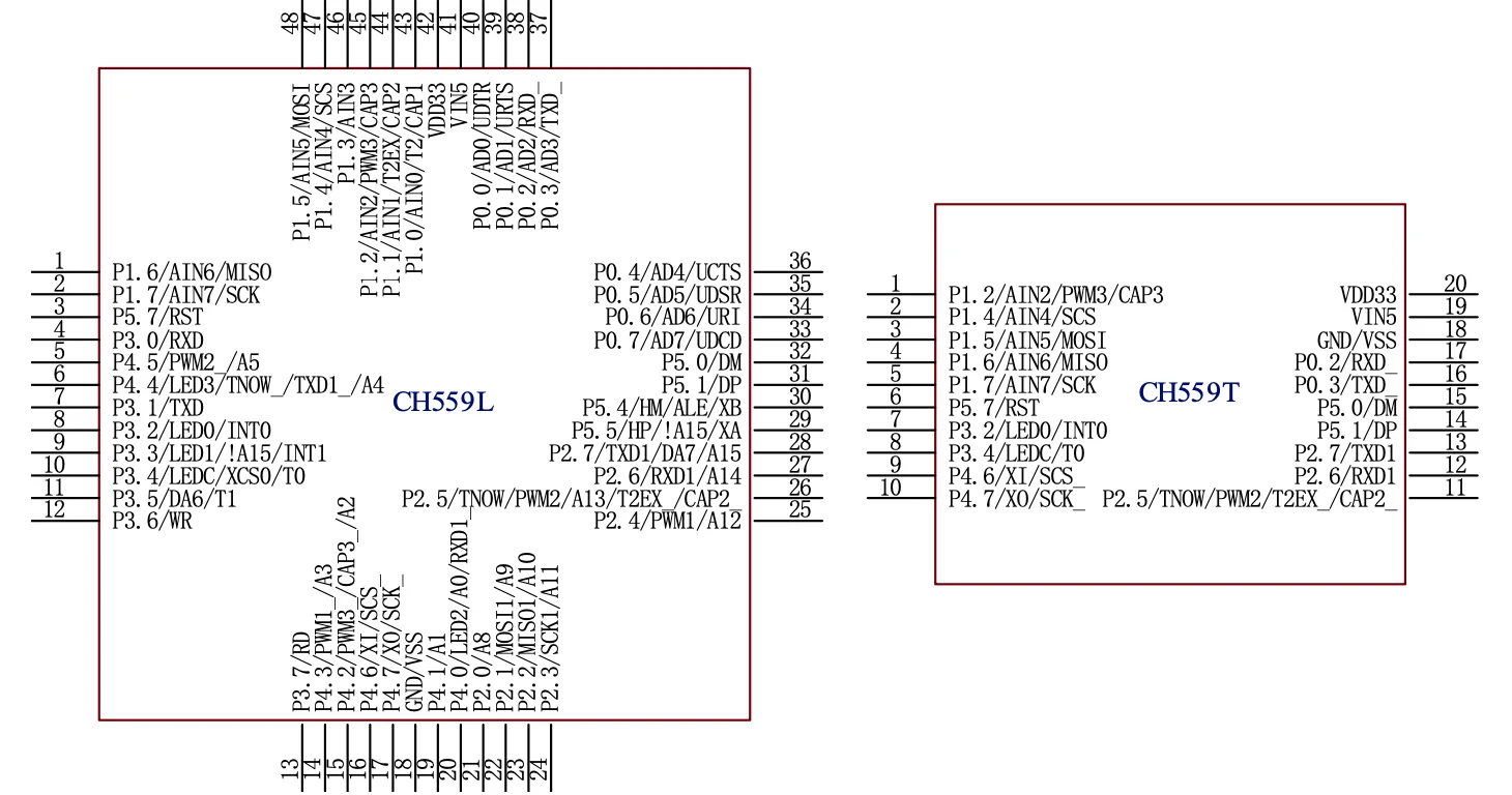
| Pin No. (LQFP48) | Pin Name | Alternate Function (Left-first priority) | Description |
|---|---|---|---|
| 1 | P1.5 | AIN5/MOSI | Default P1 port I/O, configurable as analog input channel 5, or SPI0 master output pin. |
| 2 | P1.6 | AIN6/MISO1 | Default P1 port I/O, configurable as analog input channel 6, or SPI1 slave input pin. |
| 3 | P1.7 | AIN7/SCK1 | Default P1 port I/O, configurable as analog input channel 7, or SPI1 clock pin. |
| 4 | P5.7 | RST | Default P5 port I/O, configurable as reset input pin. |
| 5 | P3.0 | RXD4 | Default P3 port I/O, configurable as UART4 receive pin, function may depend on other configuration registers. |
| 6 | P4.4 | LED3/TNOW*/TXD1*/A46 | Default P4 port I/O, configurable as LED control pin 3, timer input, UART1 transmit pin, or address bus A46 pin, function may depend on other configuration registers. |
| 7 | P3.1 | TXD7 | Default P3 port I/O, configurable as UART7 transmit pin, function may depend on other configuration registers. |
| 8 | P3.2 | LED0/INT0 | Default P3 port I/O, configurable as LED control pin 0, or external interrupt 0 input pin. |
| 9 | P3.3 | LED1/!A15/INT1 | Default P3 port I/O, configurable as LED control pin 1, address bus A15 pin, or external interrupt 1 input pin. |
| 10 | P3.4 | LEDC/XCS0/T0 | Default P3 port I/O, configurable as LED control clock pin, external bus chip select 0, or timer 0 input. |
| 11 | P3.5 | DA6/T1 | Default P3 port I/O, configurable as DAC channel 6 output pin, or timer 1 input pin. |
| 12 | P3.6 | WR | Default P3 port I/O, configurable as external bus write enable pin. |
| 13 | P3.7 | RD | Default P3 port I/O, configurable as external bus read enable pin. |
| 14 | P4.3 | PWM1_/A3 | Default P4 port I/O, configurable as PWM1 inverted output pin, or address bus A3 pin. |
| 15 | P4.2 | PWM3*/CAP3*/A2 | Default P4 port I/O, configurable as PWM3 inverted output pin, timer 3 capture input, or address bus A2 pin. |
| 16 | P4.6 | XI/SCS_ | Default P4 port I/O, configurable as external crystal input, or SPI slave chip select pin. |
| 17 | P4.7 | XO/SCK_ | Default P4 port I/O, configurable as external crystal output, or SPI clock pin. |
| 18 | GND | VSS | Ground. |
| 19 | P4.1 | A1 | Default P4 port I/O, configurable as address bus A1 pin. |
| 20 | P4.0 | LED2/A0/RXD1_ | Default P4 port I/O, configurable as LED control pin 2, address bus A0 pin, or UART1 inverted receive pin. |
| 21 | P2.0 | A8 | Default P2 port I/O, configurable as address bus A8 pin. |
| 22 | P2.1 | MOSI1/A9 | Default P2 port I/O, configurable as SPI1 master output, or address bus A9 pin. |
| 23 | P2.2 | MISO1/A10 | Default P2 port I/O, configurable as SPI1 slave input, or address bus A10 pin. |
| 24 | P2.3 | SCK1/A11 | Default P2 port I/O, configurable as SPI1 clock pin, or address bus A11 pin. |
| 25 | P2.4 | PWM1/A12 | Default P2 port I/O, configurable as PWM1 output pin, or address bus A12 pin. |
| 26 | P2.5 | TNOW/PWM2/A13/T2EX*/CAP2* | Default P2 port I/O, configurable as timer input, PWM2 output, address bus A13 pin, timer 2 external clock input, or timer 2 capture input pin. |
| 27 | P2.6 | RXD1/A14 | Default P2 port I/O, configurable as UART1 receive pin, or address bus A14 pin. |
| 28 | P2.7 | TXD1/DA7/A15 | Default P2 port I/O, configurable as UART1 transmit pin, DAC channel 7, or address bus A15 pin. |
| 29 | P5.5 | HP/!A15/XA | Default P5 port I/O, in USB Host mode as USB HUB1 port HP pin, or inverted address bus A15 pin, or RS485 differential input XA pin. |
| 30 | P5.4 | HM/ALE/XB | Default P5 port I/O, in USB Host mode as USB HUB1 port HM pin, or address latch enable ALE, or RS485 differential input XB pin. |
| 31 | P5.1 | DP | Default P5 port I/O, in USB mode as USB data line DP pin. |
| 32 | P5.0 | DM | Default P5 port I/O, in USB mode as USB data line DM pin. |
| 33 | P0.7 | AD7/UDCD | Default P0 port I/O, configurable as analog-to-digital conversion input channel 7, or USB data connection detect pin. |
| 34 | P0.6 | AD6/URI | Default P0 port I/O, configurable as analog-to-digital conversion input channel 6, or USB RI pin. |
| 35 | P0.5 | AD5/UDSR | Default P0 port I/O, configurable as analog-to-digital conversion input channel 5, or USB DSR pin. |
| 36 | P0.4 | AD4/UCTS | Default P0 port I/O, configurable as analog-to-digital conversion input channel 4, or USB CTS pin. |
| 37 | P0.3 | AD3/TXD_ | Default P0 port I/O, configurable as analog-to-digital conversion input channel 3, or UART0 inverted transmit pin. |
| 38 | P0.2 | AD2/RXD_ | Default P0 port I/O, configurable as analog-to-digital conversion input channel 2, or UART0 inverted receive pin. |
| 39 | P0.1 | AD1/URTS | Default P0 port I/O, configurable as analog-to-digital conversion input channel 1, or USB RTS pin. |
| 40 | P0.0 | AD0/UDTR | Default P0 port I/O, configurable as analog-to-digital conversion input channel 0, or USB DTR pin. |
| 41 | VIN5 | 5V external power input, powers the internal 5V-to-3.3V LDO, requires external 0.1uF decoupling capacitor. | |
| 42 | VDD33 | VDD/VCC | Internal regulator output and internal 3.3V operating power input. When supply voltage is less than 3.6V, connect VIN5 to external power. When supply voltage is greater than 3.6V, requires external 3.3uF decoupling capacitor. |
| 43 | P1.0 | AIN0/T2/CAP1 | Default P1 port I/O, configurable as analog input channel 0, timer 2 input, or timer 2 capture input pin. |
| 44 | P1.1 | AIN1/T2EX/CAP2 | Default P1 port I/O, configurable as analog input channel 1, timer 2 external clock input, or timer 2 capture input pin. |
| 45 | P1.2 | AIN2/PWM3/CAP3 | Default P1 port I/O, configurable as analog input channel 2, PWM3 output pin, or timer 3 capture input pin. |
| 46 | P1.3 | AIN3 | Default P1 port I/O, configurable as analog input channel 3. |
| 47 | P1.4 | AIN4/SCS | Default P1 port I/O, configurable as analog input channel 4, or SPI0 slave chip select pin. |
| 48 | P4.5 | PWM2_/A5 | Default P4 port I/O, configurable as PWM2 inverted output pin, or address bus A5 pin. |
Pin characteristics summary:
-
Power and ground: CH559 has independent power input (VIN5) and 3.3V operating voltage output (VDD33), as well as ground (GND) pins.
-
GPIO: P0, P1, P2, P3, P4, P5 ports are all general-purpose input/output ports, with P0-P3 ports bit-addressable.
-
Analog input: The P1 port provides 8 ADC analog input channels AIN0~AIN7 for analog signal acquisition.
-
USB:
P5.0 and P5.1 are used for USB data lines DM and DP, supporting USB Host and Device modes.
- P5.4 and P5.5 are used for USB Host’s expansion HUB1 HM and HP pins, for connecting external USB devices.
Timer/PWM: Multiple pins have timer input/output or PWM output functions, such as P1.0, P1.1, P1.2, P2.4, P2.5. UART: Multiple UART communication pins are provided, including P0.2 (RXD*), P0.3 (TXD*), P2.6 (RXD1), P2.7 (TXD1). SPI: SPI communication pins include P1.4 (SCS), P1.5 (MOSI), P1.6 (MISO), P1.7 (SCK) for SPI0, and P2.1, P2.2, P2.3 for SPI1. Reset: P5.7 (RST) is the reset pin. Crystal: P4.6 (XI) and P4.7 (XO) are for connecting external crystal oscillators.
6. Application Cases
Here are some CH559 application cases, highlighting its USB Host and Device capabilities:
- USB Host applications:
USB keyboard/mouse control: CH559 can serve as the main controller of an embedded system, connecting USB keyboards and mice through the USB Host interface for human-machine interaction. For example, it can be used to control industrial equipment or kiosks.
- USB data acquisition: CH559 can connect USB storage devices (such as USB drives), read data from them, and transfer the data to other devices or for further processing. For example, for data logging or firmware updates.
USB Device applications:
-
USB virtual serial port: CH559 can emulate a USB serial device, communicating with a PC through the USB interface, convenient for debugging and data transfer.
-
USB HID device: CH559 can implement USB HID (Human Interface Device) devices, such as USB game controllers, transmitting sensor data to a computer via USB.
Summary
The CH559 is a feature-complete, high-performance 8-bit USB microcontroller with high-speed processing capability, rich peripheral resources, and flexible USB Host/Device functionality. It has broad application prospects in industrial control, IoT, consumer electronics, and other fields. Meanwhile, WCH’s comprehensive development resources and technical support make it easier for developers to create various innovative applications with the CH559.
Hope this blog article is helpful to you!